
The measurement of the momentum of particles is crucial in helping us to build up a picture of what happens at the heart of the collision. One method to calculate the momentum of a particle is to track its path through a magnetic field; the more curved the path, the less momentum the particle had. The CMS tracker records the paths taken by charged particles by measuring their positions at a number of points.
The tracker can reconstruct the paths of high-energy muons, electrons, and charged hadrons (particles made up of quarks) as well as see tracks coming from the decay of very short-lived particles such as beauty or “b quarks” that are for example being used to study the differences between matter and antimatter.
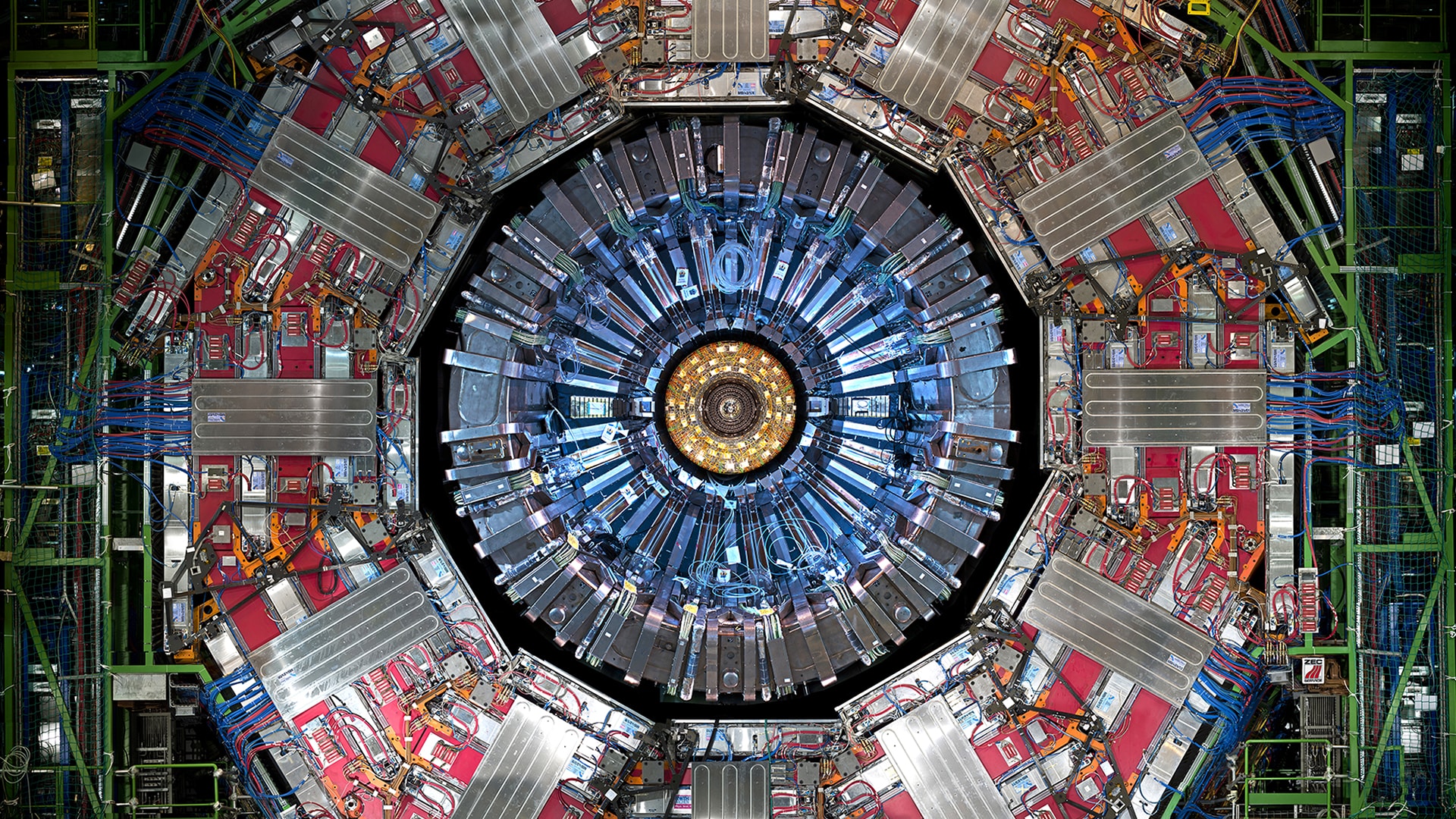
The tracker needs to record particle paths accurately yet be lightweight so as to disturb the particles as little as possible. It does this by taking position measurements so accurate that tracks can be reliably reconstructed using just a few measurement points. Each measurement is accurate to 10 µm, a fraction of the width of a human hair. It is also the innermost part of the CMS detector and so receives the highest volume of particles: the construction materials were therefore carefully chosen to resist radiation.
The final design consists of a tracker made entirely of silicon detection elements: the pixels, at the very core of the detector and dealing with the highest intensity of particles, and the silicon microstrip detectors that surround it. As particles travel through the tracker the pixels and microstrips produce tiny electric signals that are amplified and detected. The signals are stored in chips’ memory for several microseconds and then processed before being sent to a laser to be converted into infrared pulses. These are then transmitted over a 100m fibre optic cable for analysis in a radiation-free environment. The tracker uses 40,000 such fibre optic links providing a low power, lightweight way of transporting the signal. Much of the technology behind the tracker electronics came from innovation in collaboration with industry.
The tracker employs sensors covering an area the size of a tennis court, with 135 million separate electronic readout channels: in the pixel detector there are some 6600 connections per square centimetre. Silicon sensors are highly suited to receive many particles in a small space due to their fast response and good spatial resolution.
The CMS strip tracker was installed in CMS in late 2007 and has been in continuous operation since 2008. The original CMS pixel detector was operated during the years 2009 – 2016 and was replaced by the CMS Phase-1 pixel detector in an extended year-end stop 2016/2017.
Visit the link for Pixel Tracker updates: https://cms.cern/tags/tracker
More details about the CMS Tracker can be found in the following selection of documents:
The CMS experiment at the CERN LHC (paper written in ~2008 describing the original CMS experiment as build for LHC Run 1)
The CMS Phase-1 Pixel Detector Upgrade (paper from 2020 describing the Phase-1 pixel detector)
The very original description of the CMS tracking detectors can be found in the Technical Design Report (TDR) from 1998 and 2000, respectively
CMS: The Tracker Project Technical Design Report
The CMS tracker : addendum to the Technical Design Report
While many design aspects have evolved from the original concept, they still provide interesting insights about the challenges for the detectors and how they were thought to be overcome. A few more words on this are in the following paragraph.
Some design history ...
In the very first design sketch of CMS, the tracker section was left blank because it was thought that with the intensity of particles experienced in the LHC it would be impossible to make a tracker that could withstand it. In particular, making readout electronics that could work in this radiation would be a challenge. Hints that the US military, needing such electronics for space travel and nuclear warheads, might have solved some of the potential problems encouraged the team to explore this field.
However, the technology actually came from a most unexpected source; as the military market shrank at the end of the cold war and commercial electronics began to excel, the team took a gamble on a very fine feature manufacturing process, produced for a commercial market, which was not formally in the realm of “radiation hard electronics”. With some modifications, a few simple design tricks and selection of the right technology, it could be as radiation hard as needed. And it was a remarkable success. Eighteen months later the teams had rebuilt the old chips. They had low power consumption, low noise, and high overall performance and on top of this could be easily produced on a large scale, were relatively cheap and thoroughly tested. It was a big breakthrough. The same technology was then also used for the ECAL as well as CMS and ATLAS pixels.
- Printer-friendly version
- Log in to post comments


